Third Time Lucky
Student experience 15th February 2016
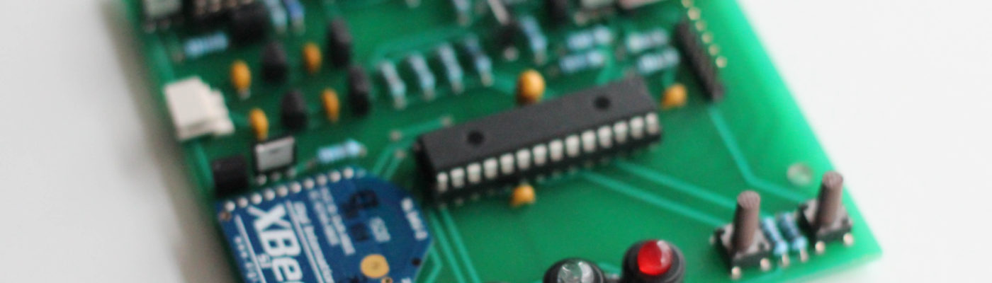
This week has been a momentous step in the hardware side of the project. After weeks of prototyping the entire system on breadboard (some said this was impossible), the circuit is finally at a finalised stage.
Weeks of slight changes, and many factors still to be decided, meant this stage has come a lot later than I’d hoped. The PCB essentially draws the line on the final circuit, with it being virtually impossible to make any changes after this point. It’s now done, but it didn’t go too smoothly.
FIRST TIME AROUND
The first thing I learnt about real PCB design is that I’m expected to do a lot of the work. After years of being used to library components and footprints, suddenly this wasn’t the case. Basic components such as resistors have a stock footprint, meaning a straight transfer from the circuit diagram to the PCB. The use of more ‘exotic’ components, such as specific modules, chips and diodes, aren’t however stock.
This means designing a schematic / footprint for each of these devices (consisting of around half the unique components used). It’s fair to say this didn’t go to plan first time around.
Issues including mounting holes being too small and incorrect pin mappings meant version 1.0 was a write off. Back to the design file, amendments were made, but version 1.1 didn’t even make it to production. The PCB office rejected the design for violating a few manufacturing requirements (issues with pad sizes and routing constraints).
‘FAVOURITE TOY’
Finally, version 1.2 was completed and ready to be populated (all the components fitted). In the context of Electronic Engineering, if 3rd Year Project is the ‘dream’ every child has, then populating a PCB is every child’s ‘favourite toy’. Finding and soldering components is just about the most fun you can have as an electronic engineer.
At the time of writing, there’s a couple of components missing, preventing testing the PCB. In due course it will be tested, and fingers crossed it’ll work!

Leave a Reply